The ZX-Spectrum ZXMMC Interface's page
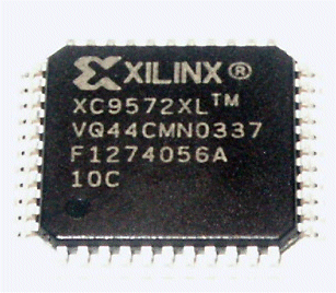
The project fits into a Xilinx's 36 macrocells XC9536XL 3.3V cpld, 5V tolerant (the photo shows the XC9572XL, 72 macrocells, VQ44 package). These components are well suited for interfacing the 5V ZX-Spectrum logic to 3.3V sd/mmc card logic.
After programming through the JTAG header, the XC9536XL CPLD will work as an SPI device at these addresses:
$1F: WR Only = 2 bit chip select register (D0 =
MMC0; D1 = MMC1), active LOW
$3F: RD/WR = SPI TX/RX Register (8 bit).
The card chip select logic has a built in protection that prevents enabling both cards at the same time.
If a larger (XC9572XL) CPLD is installed, then the interface will provide a Kempston Joystick port and an hardware RS-232 115K2 baud serial port. It should be noted that rs-232 communication can be disturbed if ULA suspends the Z80 clock for any reason, as this is the CPLD clock as well. SD/MMC card data transfer is not affected as the SPI port is synchronous type.
Port List for the FULL version (9572 cpld only):
$1F: RD = KEMPSTON (5 bit, '1' = input active);
WR = card CS (D0 = MMC0; D1 = MMC1); D3 = NMI enable: 1 = NMI is
issued on RS-232 RX
$3F: RD/WR = SPI TX/RX Register (8 bit)
$5F: RD = read RS232 status (5 bit)
$7F: RD/WR = RS-232 TX/RX Register (8 bit).
STATUS REGISTER ($5F):
D0: 0 = receiver empty; 1 = receiver has data
D1: 0 = no error; 1 = overrun
D2: 0 = no error; 1 = framing error
D3: 0 = transmitter idle (ready); 1 =
transmitter full
D4: 0 = receiver idle; 1 = reception is in
progress (but not completed yet)
In current version, the Kempston port can be enabled/disabled by
means of a jumper to be placed on RS-232 connector between GND and
the ex-DTR pin, now "kempston enable". NOTE: the new kempston
enable pin should be tied to +VDD by a pullup resistor; luckily,
there is a spare one in the 10K resistor network.
If an XC9572 (larger) CPLD is installed but the user wants to drop the additional features (Kempston and rs-232) an alternate Jedec file can be programmed, turning it into an equivalent of the XC9536 version. Please note that in this case, CPLD still has WRITE ENABLED on all ports. This means that a byte written to port $7F will be sent through the rs-232 TX pin, while READ is disabled on all ports except $3F (SPI port).
When the processor reads one of the above I/O ports for the 9572 full version, or the SPI port for the standard version, the corresponding data is placed on databus.
When the processor writes to one of the above I/O ports, or the SPI port for the XC9536 version, then the CPLD starts an internal counter that latches databus status into proper internal register on the falling edge of T3 cycle, which is right in the middle of the write operation. Since IORQ and WR are issued on the rising edge of main clock (on T2), the internal logic (counter and latches) works on falling edge in order to guarantee reliability in the count process.
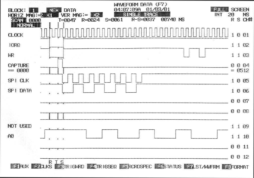
The following diagram shows a write cycle to port $3F, which is the SPI OUT register, for the PREVIOUS version (17T-states) of the SPI section. For debug purposes, a "capture" signal has been configured on the CS1 pin (unused), that goes high when data is latched (which happens on the falling edge of T3 cycle, as stated above). The byte written to port $3F is "$55":
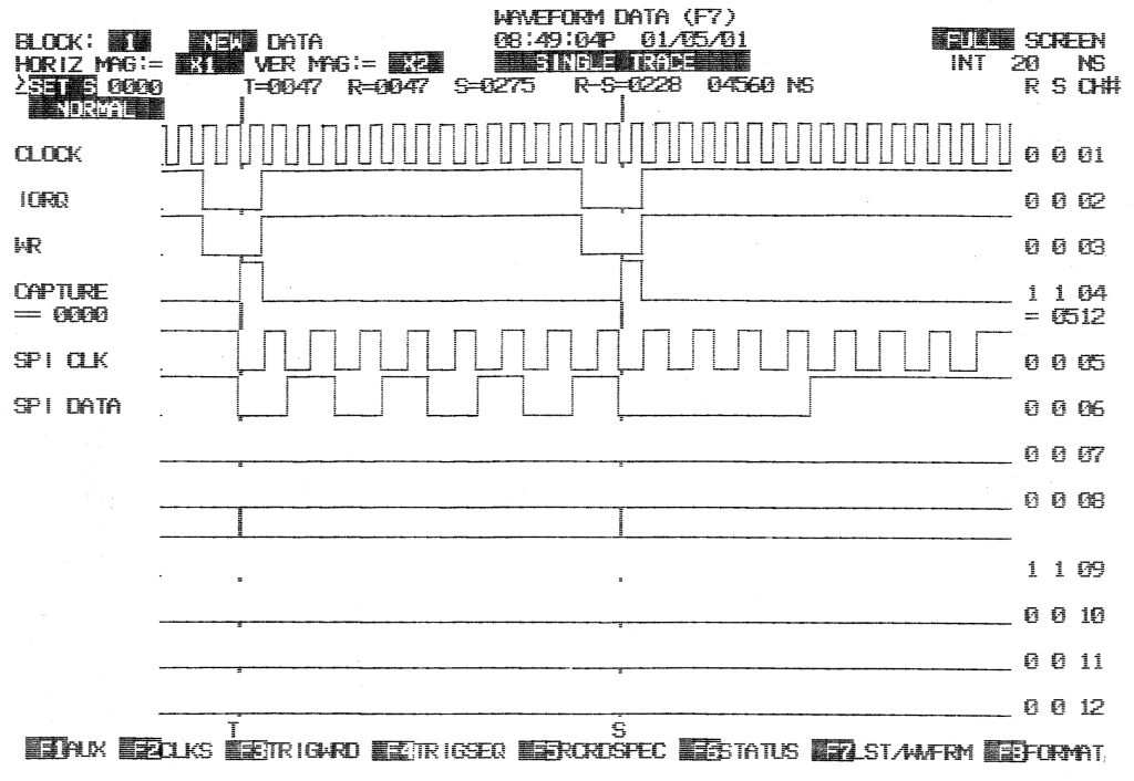
This is the NEW 16T-states version: to achieve this speed, SPI cycle begins while the processor is still in the middle of the WR operation.
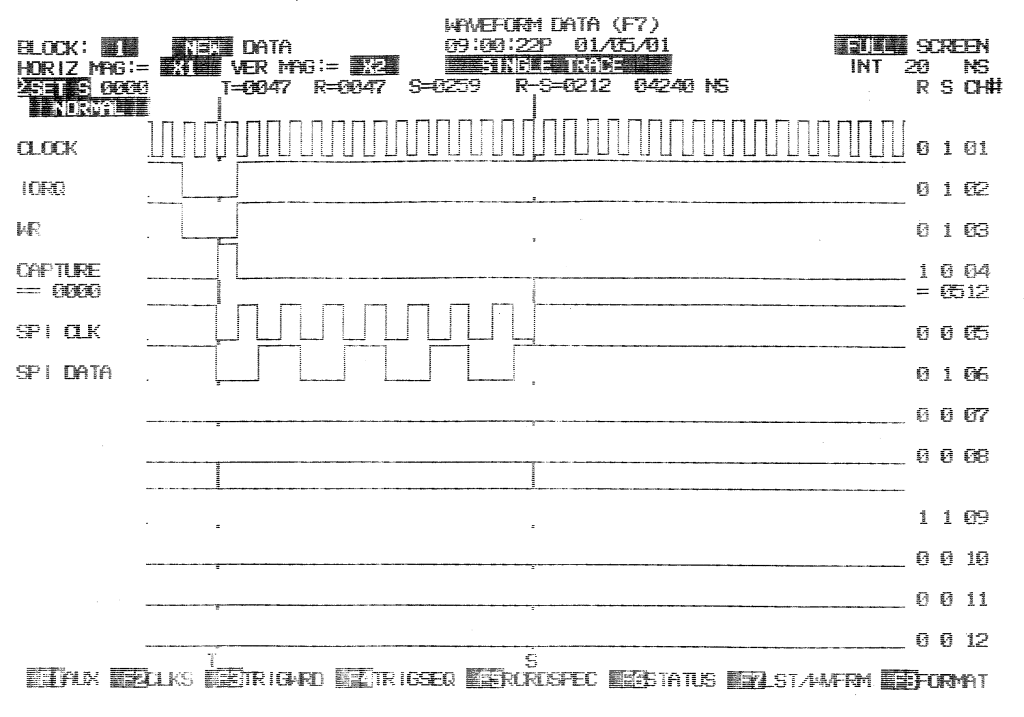
Thanks to this improvement, which saves one T-state, OUTI (16T) instructions can now be used. The result is a continuous data flow, as shown in the following diagram, where two bytes are written by two consecutive OUTI with $55 and $0F data:
JEDEC Programming file for Standard XC9536XL version, compiled with ISE Webpack 9.1 SP1
JEDEC Programming file for 9572XL standard version (works as the XC9536 version), ISE 9.1 SP1
JEDEC Programming file for
9572XL Full Version, ISE 9.1 SP1